1

I'm planning to control 3 LEDs and a heating element (5 Ohms) using a Raspberry Pi.

The main power supply outputs 12V & 5A. Using an L78S05CV Voltage regulator, I'm planning to power the RPi. So far I didn't decide how I'm gonna power the heating element. I mean, It could possibly use either the 5V or the 12V.

Anyway, in order to switch on and off the heater, I searched for some logic-level MOSFETs and calculated the power dissipation (P) that the heater will cause to the MOSFET as well as the maximum MOSFET dissipation without using a heatsink (Pd).

Here is a gathering table of what I've found and calculated so far:

+-------------+-------------+----------+---------------------+--------+
|   MOSFET    | VGS(th) (V) | P@5V (W) |      P@12V (W)      | Pd (W) |
+-------------+-------------+----------+---------------------+--------+
| IRLB8743PbF | 1.35 - 2.35 |   0.0032 | 0.018               |   2.41 |
| IRL540      | 1.00 - 2.00 |    0.077 | 0.443               |   2.41 |
| FDN337N     | 0.40 - 1.00 |    0.065 | 0.374               |    0.5 |
| IRLD014     | 1.00 - 2.00 |    0.200 | 1.152(needs a sink) |   1.25 |
| IRLZ44N     | 1.00 - 2.00 |    0.025 | 0.126               |   2.41 |
+-------------+-------------+----------+---------------------+--------+

So, since I'm new to this I would like to ask for your opinion on which one or maybe more than one is better for that case.

Maybe my approach is totally wrong and these calculations make no sense in such a project. So any idea hint or other suggestion is welcome.

EDIT

I've added two schematics on how I'm imagining the circuit (maybe I've missed any capacitors around the MOSFET). Anyway. The first one is driving the heater element using 12V while the other using 5V.
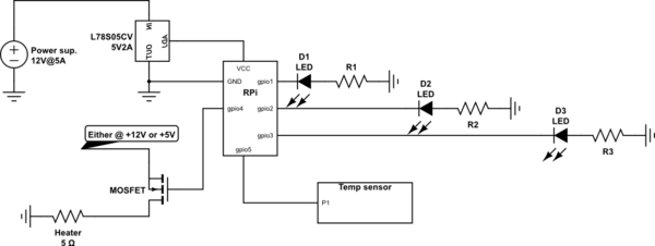
schematic

simulate this circuit – Schematic created using CircuitLab

EDIT 2 I edited the schematic and I think I fixed the issues mentioned earlier from @Dmitry Grigoryev.

3
  • Hi @J.Doe, Welcome and nice to meet you. Your research notes on power MOSFET is good. I happened to have also done some tests on the same subject. My interest area is a bit different from you so is my approach. Now let me make some quick comments: (1) As you did, first thing first is Vgs(th). The reason is that most old generations eg IRF504N have high Vgs around 7V. So we need to find low Vgs, (2) What you do not emphasize is switching current. I need to switch current from 500mA to 50A, but luckily power MOSFET can entertain big current happily. / to continue, ...
    – tlfong01
    Commented Nov 23, 2019 at 1:44
  • Their On Resistance is very small, comparing with power NPN Darington such as TIP120. So there is no worry of using bulky heat sink. (3) I have been using the old IRF540N, so my new replacement is IRL540N. (4) I should have forgotten perhaps other important points. So you might like to skim my old posts on IRL540N and feel free ask me any newbie questions! :) And here is my IRL540N Engineering Experimentation Notes: penzu.com/p/d9fef62f
    – tlfong01
    Commented Nov 23, 2019 at 1:51
  • One thing that might puzzle you is that my goal is to turn on/off home heater of 200VAC/DC (or 10A 2000W), but I am using only low voltage 12VDC (and very low resistor) to switch high current. As I said, what is important is the current, never mind the voltage 200VDC or 12VDC. So 12VDC is good for experimentation.
    – tlfong01
    Commented Nov 23, 2019 at 2:00

2 Answers 2

3

I'm a bit unclear on your exact question, but here's a couple of thoughts based on what it seems you're trying to do:

Re. power dissipation in a semiconductor:

You may be all over this already, and if so, please excuse me for being pedantic, but the important thing in selecting a semiconductor (MOSFET in this case) for a power switching application is junction temperature. You must make sure you don't overheat the device, otherwise you will destroy it in short order. If you're not familiar with these calculations, they're not difficult, but you will need to make sure you're using the appropriate value from the device's spec sheet. The calculation itself involves three parameters:

  1. power dissipation (PD): All MOSFETs have some 'on-state' resistance (RDS) between the drain and source terminals, and therefore they will dissipate some of the power delivered by your source as heat. The dissipation is application dependent, and you must calculate it. If you know the RDS value, and the amount of current your MOSFET will pass to the load (IL), you may calculate the approximate PD by:

PD = IL2 * RDS

  1. ambient temperature (TA): This is simply the temperature of the environment in which your MOSFET operates.

  2. thermal resistance from junction to ambient (RJ-A): This is simply the measure of how well the MOSFET's case (and heat sink if you use one) is able to conduct the heat generated at the junction to the ambient outside the case. This value is given in the spec sheet for the device.

Once you have these 3 values, you can calculate an approximation to the MOSFET's junction temperature:

TJ = TA + PD * RJ-A

You may also wish to use one of several 'online' calculators to perform this calculation for you.

In any event, you must keep your MOSFET's junction temperature within a safe operating area for good performance and reliability. This is a fundamental part of the design.

Re. driving a MOSFET from the RPi GPIO:

This is never a good idea, especially for a power switching application. The GPIO pins are rated for 3.3V and will source (or sink) a few milliamps of current (ref). Even the so-called 'logic level' MOSFETs operate poorly (slow turn-on & high RDS) when driven at these levels.

Instead, drive a Darlington pair bipolar transistor from the GPIO, and drive the MOSFET's gate with the Darlington transistor. As an example, here's a schematic showing how to drive a relay with a Darlington transistor. In your case, you will drive a MOSFET instead of a relay coil!

If you're interested in this (Darlington) approach, please edit your question and add a schematic to show us your power supplies, LEDs, heating elements and RPi. We'll be able to help you with details of a design once we know your objectives.

1
  • I've edited with some schematics you requested. I hope they are easy to read.
    – J. Doe
    Commented Nov 25, 2019 at 12:35
2

I just wanted to draw your attention to the fact that your schematics will not work and will likely kill your electronics.

In your first schematic, you apply +12V to RPi GPIO pins (through R1, D1 path) which will kill the RPi.

In your second schematic, the 12V power supply is wired in a way that produces 0V on the (+) terminal and -12V on the (-). As a result your RPi will never get powered at all because it can only work with positive voltage.

In both schematics, your voltage regulator is wired in a way that applies a constant voltage (either 12V or -12V) across it, so there's nothing it can regulate. Forcing +12V over a 5V regulator will quickly destroy it, not sure about the case of reverse polarity.

2
  • 1
    Ok. You're right. I draw them very quickly due to a lack of time. I will change and update them. Thanks.
    – J. Doe
    Commented Nov 25, 2019 at 13:16
  • FYI I've edited the schematic. Now I think makes more sense.
    – J. Doe
    Commented Nov 26, 2019 at 15:56

Your Answer

By clicking “Post Your Answer”, you agree to our terms of service and acknowledge you have read our privacy policy.

Not the answer you're looking for? Browse other questions tagged or ask your own question.