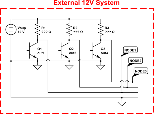
Your question is a bit unclear to me. Let's first try to define the problem clearly; the answer should fall out easily after that. Below is a schematic (created using RPi SE's invaluable tool). From the description in your question, I imagine this is how it is designed:
Three independent binary outputs that switch between 12VDC and GROUND. Note the presence of a pullup resistor (R1, R2, R3) on each channel. When the transistor (Q1, Q2 or Q3) is turned OFF, and with nothing connected to the output (Node1, Node2 or Node3) a voltmeter will read 12VDC.

simulate this circuit – Schematic created using CircuitLab
You will need to verify whether the above schematic is accurate - or not. This may be accomplished simply if you have a voltmeter (use LEDs otherwise):
- Remove all connections from the outputs (Node1, Node2 & Node3).
- Measure the voltage between Node1 and GND; repeat for Node2 & Node3
- ADJUST the input to your system, and repeat Step 2
Case I
If the voltages at Nodes1-3 are never different from each other, your external system's outputs are not independent, and there's nothing you can do with the RPi to make them behave differently.
Case II
If the voltages at Nodes1-3 are different from each other, and dependent upon the external system's inputs, you have mis-wired something, and the schematic you've provided is either incorrect or incomplete.
Having sorted that, your next step is to design a proper interface between the RPi GPIO pins; proper being an interface that provides approximately 3.3V output when the external system's output (Node1, 2 or 3) is 12V, and approximately 0V (relative to GND).
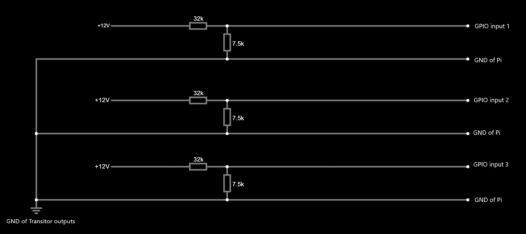
The voltage divider interface you've adopted in your schematic is only one (of many) possible interfaces. Some alternatives to the voltage divider are listed in another answer here, and may be useful in your case. The primary issue in designing a proper interface to an external system that uses a pullup resistor is that some of the interfaces require you to account for the pullup resistor's value in design of the interface. Consider the use of a Zener diode interface to simplify that design.


