This post doesn't add much fundamentally new information, but it does (1) give a step-by-step visual guide, and (2) document the process for an older Pi 1 B with the "P5" header.
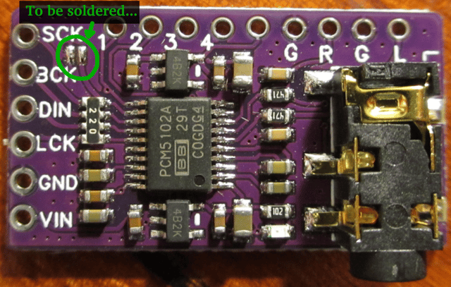
Here's how my DAC arrived — notice none of the pads are soldered, unlike most of the pictures you see online.


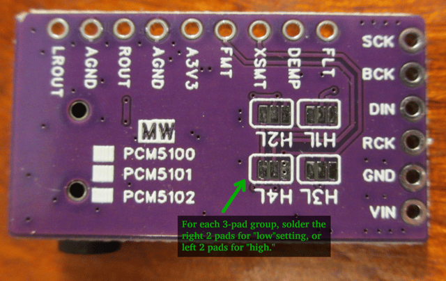
As the other answers note, the 3-pad groupings are used to select functionality for the DAC.
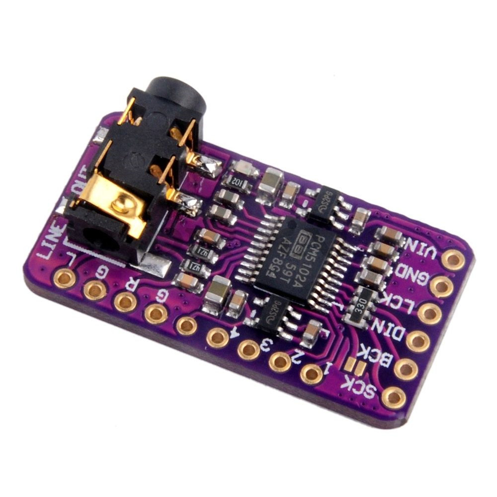
Using the labeling on my board, we want:
- H1L: FLT — "low" for normal latency filter
- H2L: DEMP — "low" to disable
- H3L: XSMT — "high" to disable
- H4L: FMT — "low" for I2S
A later picture will show these.
Aside: For soldering the pads, I found it very useful to "paint" the desired 2 pads with flux. Then, the solder flows nicely onto them and avoids the other unwanted pad. They are pretty small, so it's a little fussy to get right.
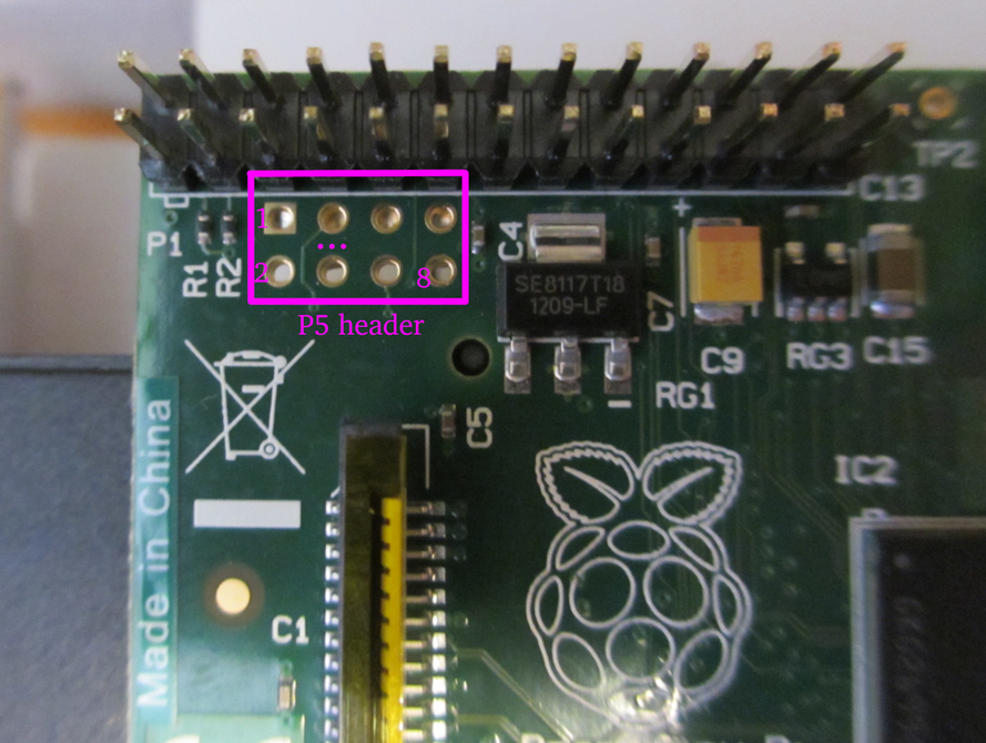
Next, here is my Raspberry Pi board, showing the P5 header that we'll use.

The P5 header is fairly well-documented here: https://www.raspberrypi-spy.co.uk/2012/09/raspberry-pi-p5-header/
There is some more good info in the original announcement from 2012: https://web.archive.org/web/20121021133116/http://www.raspberrypi.org/archives/1929
In particular, they say:
This carries the four GPIO signals [BCM2835/GPIO28 – BCM2835/GPIO31]
named GPIO7 – GPIO10 respectively, along with +5V0, +3V3 and two 0V.
Currently this connector is not populated.
...
This GPIO allocation provides access to one of:
- SDA0, SCL0 (Operating independently of P1 SDA1, SCL1); or
- PCM_CLK, PCM_FS, PCM_DIN, PCM_DOUT or I2S; or
- Four GPIO signals.
So, for an audio application like this, these are the pin functions:
- Pin 1: +5V
- Pin 2: +3.3V
- Pin 3: GPIO28 / PCM_CLK
- Pin 4: GPIO29 / PCM_FS
- Pin 5: GPIO30 / PCM_DIN
- Pin 6: GPIO31 / PCM_DOUT
- Pin 7: 0V Ground
- Pin 8: 0V Ground
We won't use PCM_DIN, since that's for input (eg: a microphone).
We also won't use 3.3V or the other Ground; thus we'll use 5 pins total (1,3,4,6,8). Note: as mentioned in other answers, the DAC internally uses 3.3V, but has a voltage regulator so can take 5V as input. So, probably either will work; I used 5V.
Aside: I'm not really sure the difference between PCM_xxx and I2S. On the DAC, we'll set its mode to I2S, but the pinout on the Pi matches PCM_xxx usage. I'm not sure why in the original release notes they said "PCM_xxx ... or I2S". Maybe they mean "also referred to as ..." ?
Confusing terminology:
The pin names are a little sloppy between the DAC and the Pi (and apparently everywhere in electronics, to be fair). If you look at the I2S Wikipedia page, you'll see some "official" names for things, but they're often not used, or even mis-used! More good info at this site: https://infocenter.nordicsemi.com/index.jsp?topic=%2Fcom.nordic.infocenter.nrf52832.ps.v1.1%2Fi2s.html
So, here's how things line up:
| Pi name |
DAC name |
Official Name |
Notes |
| CLK |
BCK |
"continuous serial clock" (SCK). Typically written "bit clock" (BCLK). |
Despite the official "SCK" designation, this does NOT match the "SCK" pin on the DAC. Ugh. |
| FS |
LCK |
"word select" (WS). Typically called "left-right clock (LRCLK) or "frame sync" (FS) |
|
| DOUT |
DIN |
"serial data" (SD), but can be called SDATA, SDIN, SDOUT, DACDAT, ADCDAT, etc. |
We connect the Pi's DOUT to the DAC's DIN. The Pi also has an (unused) DIN. The DAC does not have a DOUT. |
Note: we do not use the "SCK" pin on the DAC. As noted in other answers, we solder the pad just next to it, which causes the board to use an internal timer. This corresponds to the optional "master clock" mentioned on Wikipedia — it is not part of the I2S standard. It is sometimes written MCK.
Okay, so with that in mind, lets get wiring.
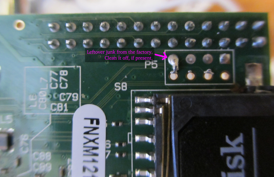
Note: my Pi had some crud on bottom of the P5 header, which I cleaned off before proceeding. I think it was safe as-is, since the shorted-out part was just the two Ground pins, but just being tidy:

Not pictured: I soldered pin headers onto the Pi's P5 header and the DAC's 5 pin holes we'll use. Again, flux is your friend.
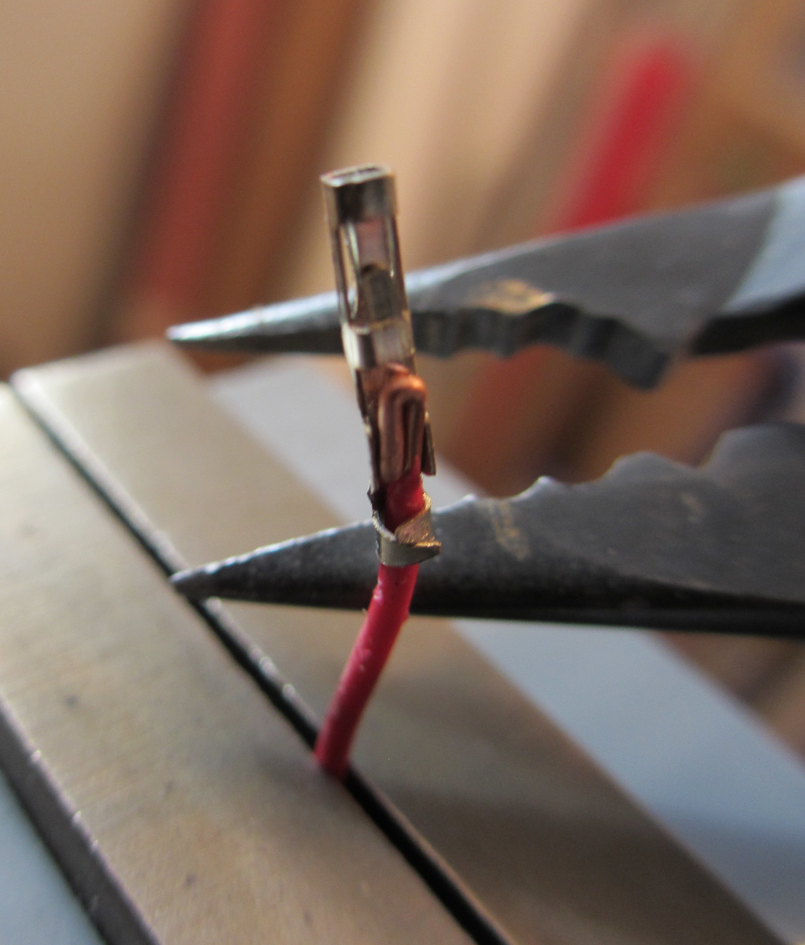
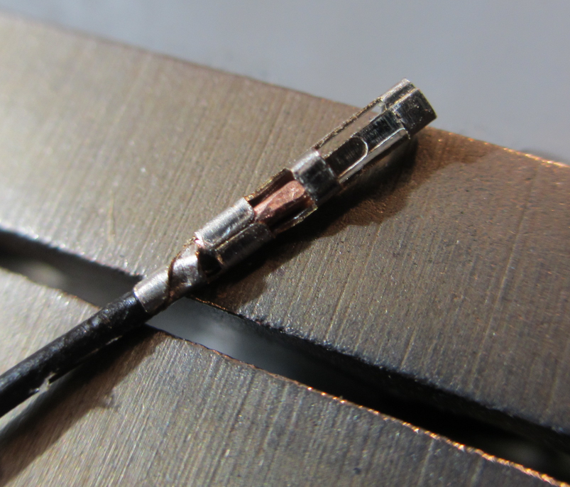
I used some jewelery pliars to do the crimping of the wire terminals — I don't have the proper tool for that. They worked okay.
Work in progress:

A decent terminal:

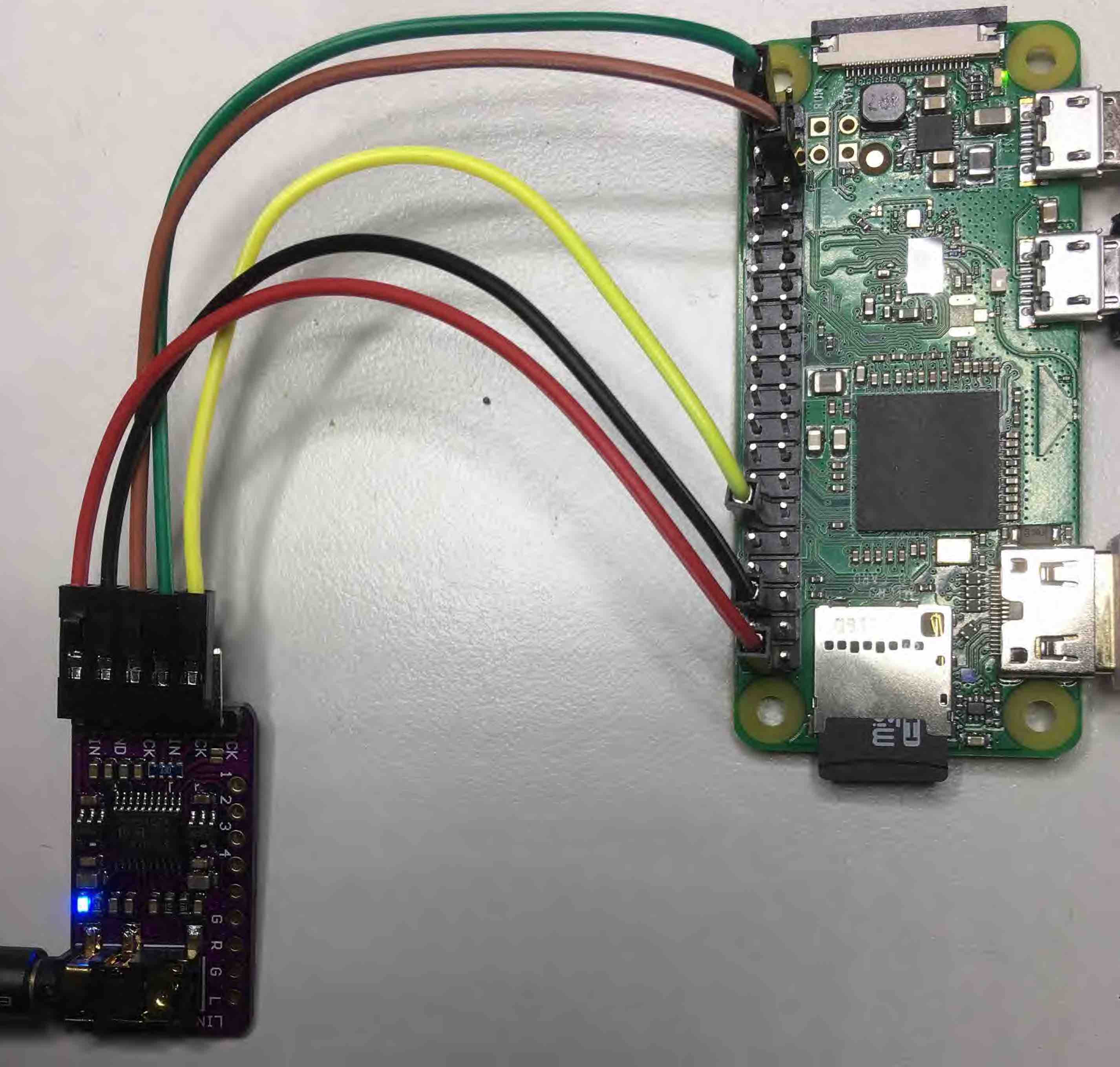
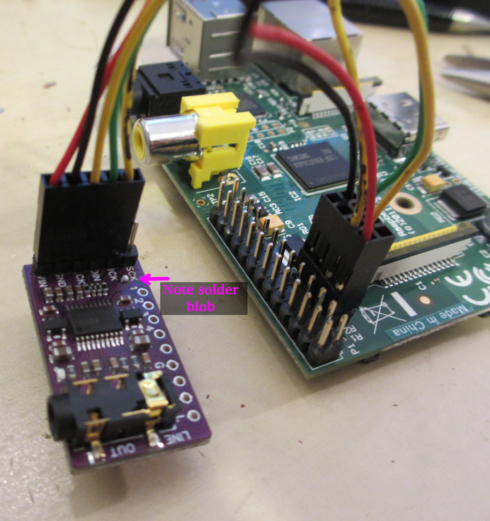
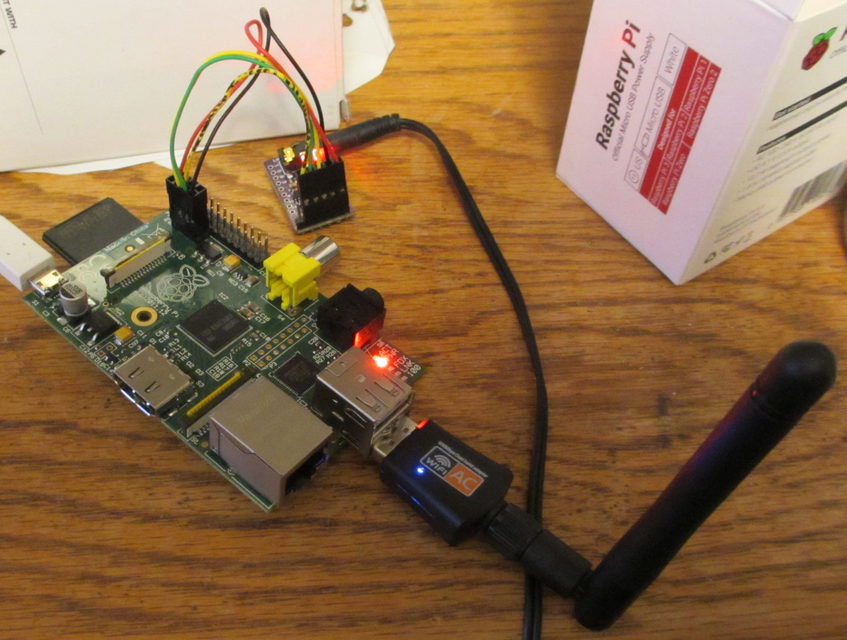
Here it is all hooked up:

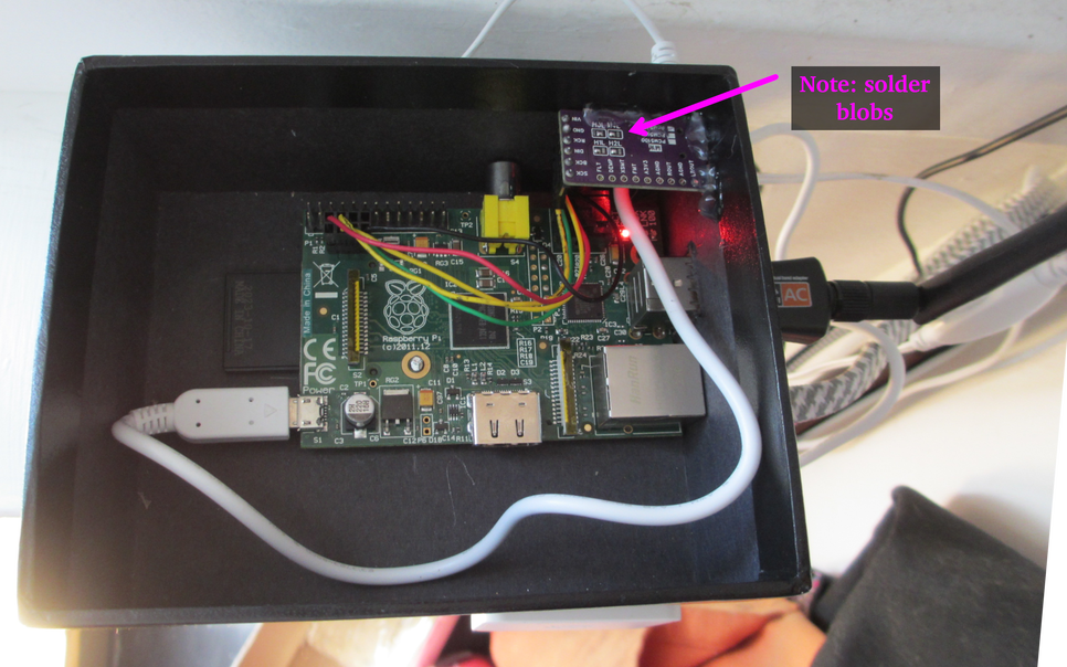
Note the SCK solder blob.
For reference, these are the wire colors corresponding to the pins:
| Color |
DAC pin |
Pi Pin |
Meaning |
| Red |
VIN |
5V |
+5V power |
| Black |
GND |
Ground |
0V Ground |
| Yellow |
LCK |
PCM_FS |
word select/frame sync clock |
| Green |
DIN |
PCM_DOUT |
serial data |
| Yellow+Black |
BCK |
PCM_CLK |
bit clock |
And plugged in with power, WiFi, etc (the DAC has a solid red LED when properly powered):

And then put in a box:

Note the solder blobs for H1L–H4L.
Also: I like hot glue.
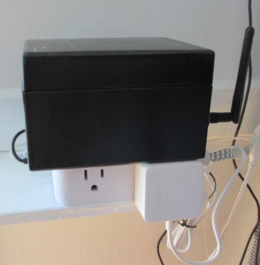
And finally put to use!

A little janky, but it works (:
Not shown here: I installed piCorePlayer and configured it to be a headless player for my home's audio.
Getting the driver for the WiFi USB dongle was a small chore (documented here: https://forums.slimdevices.com/forum/user-forums/linux-unix/1716902-success-building-wireless-driver-for-picoreplayer-rtl8821cu#post1716902), but it's all working now.
In the future I'll add some GPIO buttons and maybe some LEDs, but this gets it essentially working.
I hope it helps!
 What is the Device Driver / Device Setup

