Question
I2C device reading writing errors problem. How to solve it?
Answer
There are many reasons causing reading and writing errors. To name a few:
Wires too long (more than 30cm) and not twisted. A suggestion is to use twisted cable Cat 5 to reduce mains EMI noise picking up,
I2C speed too high. A suggestion it to start testing a low speed, such as 100kHz,
Pullup overloading Rpi which already has 1k8 pull up. A suggestion is to remove ALL pullups of the I2C devices,
Rpi I2C circuit too noisy. A suggestion is to use logical level converters such as TXS010n, TXB010n to step up 3V3 signal to 5V (high level means low risk of noise etc problem)
PSU dirty. A suggestion is to place standard bypass/decoupling cpas 10u tantalum and 0.1 ceramic near the device and also near the Rpi mciro USB connector.


/ to continue, ...
References
I2C Manual - Application Note AN10216-01 - NXP
I2C Bus Pullup Resistor Calculation - Application Report SLVA689–February 2015 - TI
Clean Power for Every IC, Part 1: Understanding Bypass Capacitors - Robert Keim, AAC 2015sep21
Clean Power for Every IC, Part 2: Choosing and Using Your Bypass Capacitors - Robert Keim. AAC 2015sep27
Introduction
It is not inconceivable that a dedicated, successful engineering
student would graduate from college knowing almost nothing about one
of the most pervasive and important components found in real circuits:
the bypass capacitor. Even experienced engineers may not fully
understand why they include 0.1 µF ceramic capacitors next to every
power pin of every IC in every circuit board they design. This article
provides information that will help you to understand why bypass
capacitors are necessary and how they improve circuit performance, and
a follow-up article will focus on details related to choosing bypass
capacitors and the PCB layout techniques that maximize their efficacy.
...
Solution
it is convenient that such a serious problem can be effectively
resolved with a simple, widely available component. But why the
capacitor? A straightforward explanation is the following: A capacitor
stores charge that can be supplied to the IC with very low series
resistance and very low series inductance. Thus, transient currents
can be supplied from the bypass capacitor (through minimal resistance
and inductance) instead of from the power line (through comparatively
large resistance and inductance). To better understand this, we need
to review some basic concepts related to how a capacitor affects a
circuit.
First, though, a brief note about terminology: The components
discussed in this article are regularly referred to as both “bypass
capacitors” and “decoupling capacitors.” There is a subtle distinction
here—“decoupling” refers to reducing the degree to which one part of a
circuit influences another, and “bypass” refers to providing a
low-impedance path that allows noise to “pass by” an IC on its way to
the ground node. Both terms can be correctly used because a
bypass/decoupling capacitor accomplishes both tasks. In this article,
however, “bypass capacitor” is favored in order to avoid confusion
with a series decoupling capacitor used to block the DC component of a
signal.
A Standard Approach
The foregoing analysis helps us to understand a classic bypassing
scheme:
a 10 µF capacitor within an inch or two of the IC, and
a 0.1 µF ceramic capacitor as close to the power pin as possible:
The larger capacitor smooths out lower-frequency variations in the
supply voltage, and the smaller capacitor more effectively filters out
high-frequency noise on the power line.
If we incorporate these bypass capacitors into the 8-inverter
simulation discussed above, the ringing is eliminated and the
magnitude of the voltage disturbance is reduced from 1 mV to 20 µV,
...
Update 2019may04hkt0846
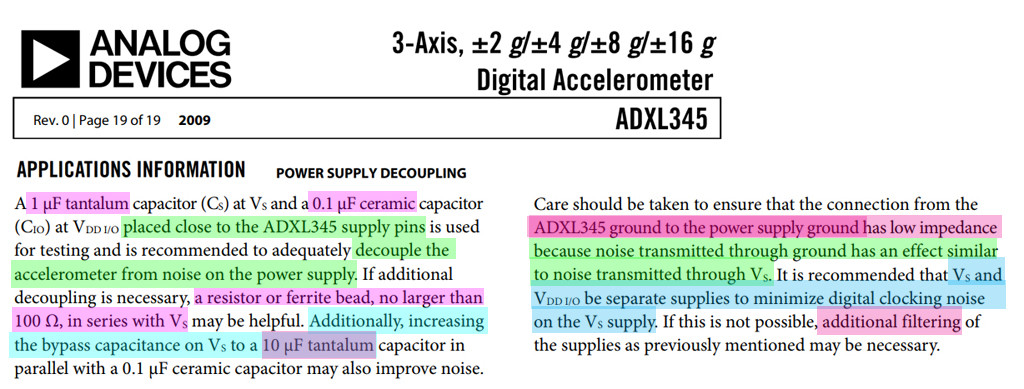
Grounding is also a problem. See the ADXL346 Datasheet's suggestion below.


